ASIC Design Flow for Protocol-Rich SOCs
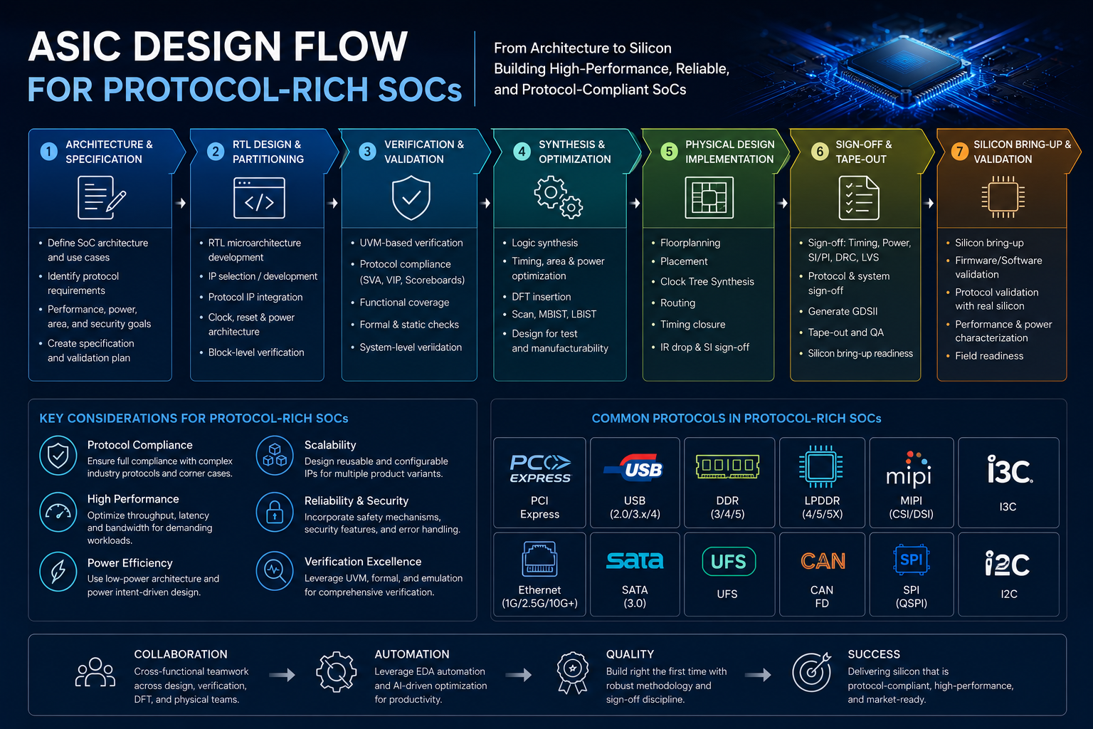
A structured, phase-gated design flow is the foundation of every successful tape-out. SSN engineers are proficient across all stages — from microarchitecture specification to final GDS-II signoff — with deep expertise in the unique challenges posed by SOCs integrating PCIe, Ethernet, AMBA, SerDes, and other high-speed protocols.
Modern SOC design is not a linear waterfall. It is an iterative, heavily parallelized process in which verification, synthesis, DFT, and physical design activities overlap and feed back into each other. SSN’s design flow methodology is adapted from industry-standard practices used at Tier-1 semiconductor companies, refined through hands-on delivery of multi-protocol ASICs in telecom, networking, and automotive applications.
The 12-Stage ASIC Design Flow
Stage | Activity |
Stage 1 | Product Specification & Micro-Architecture |
Stage 2 | RTL Design & IP Integration |
Stage 3 | RTL Functional Verification (UVM/SV) |
Stage 4 | Synthesis & Technology Mapping |
Stage 5 | Static Timing Analysis (STA) — Pre-Layout |
Stage 6 | Design for Testability (DFT) |
Stage 7 | Physical Design — Floorplanning |
Stage 8 | Physical Design — Placement & Clock Tree Synthesis |
Stage 9 | Physical Design — Routing & Signal Integrity |
Stage 10 | Static Timing Analysis (STA) — Post-Layout Signoff |
Stage 11 | Physical Verification: DRC / LVS / ERC / EM |
Stage 12 | GDSII Tapeout & Post-Silicon Bring-Up |
Stage 1 — Product Specification & Micro-Architecture
Every successful SOC begins with a precisely defined micro-architecture specification. Ambiguity at this stage propagates into RTL bugs, re-spins, and schedule overruns. SSN’s architecture team produces the following artifacts before RTL coding begins:
- System Requirements Document (SRD) — functional requirements, performance targets (throughput, latency, power budget), and interface contracts for each protocol domain.
- Micro-Architecture Specification (MAS) — block-level descriptions, datapath widths, pipeline depths, FIFO sizing, clock domains, and reset topology.
- Interface Contract Documents — signal-level specification for every chip boundary: PCIe SERDES interface, Ethernet SGMII/XGMII/CAUI, AMBA bus widths, and pad ring allocation.
- Register Map Specification — IP-XACT 2014 compliant register definitions, exported to UVM RAL and documentation simultaneously.
- Verification Planning — coverage model, simulation strategy (block-level vs. chip-level), emulation requirements, and VIP procurement list.
Protocol Micro-Architecture Considerations PCIe: Define TLP buffer sizing, LTSSM power state policy, AER register map, and MSI-X table allocation. Ethernet: Define MAC FIFO depths, PCS lane count, RS-FEC enable/disable straps, and management interface (MDIO/XSBI). AMBA: Size AXI NoC bandwidth (per-master read/write channels), define QoS priority levels, specify AXI-to-APB bridge latency budget. SerDes: Define CDR reference clock architecture, equalization algorithm, lane bonding policy, and BIST loopback modes. |
Stage 2 — RTL Design & IP Integration
SSN’s RTL engineers deliver synthesizable, lint-clean, CDC-safe SystemVerilog code that is designed to be verified efficiently. The ‘verification-friendly design’ principle — observable internal states, controllable reset paths, and clearly commented clock domain boundaries — is enforced by code review from day one.
IP Development
For custom IP blocks (protocol controllers, DMA engines, datapath accelerators), SSN follows a structured RTL development flow:
- RTL coded in synthesizable SystemVerilog, targeting the foundry PDK and the client’s chosen EDA toolchain.
- Coding guidelines enforced: no latches, no combinational feedback loops, all asynchronous signals synchronized at clock domain boundaries, all resets qualified.
- Linting run daily using Synopsys SpyGlass (GoodDesign + GoodClockReset rule sets). Zero lint errors before handoff to verification.
- CDC analysis using SpyGlass CDC or Cadence Conformal CDC — all multi-bit CDC paths have gray-code or handshake synchronizers; formal proof produced for every CDC crossing.
Third-Party IP Integration
Most protocol-rich SOCs incorporate hard IP (SerDes PHY, DDR PHY, PLL) and soft IP (PCIe controller, Ethernet MAC) from ARM, Synopsys, Cadence, or the foundry. SSN’s IP integration methodology addresses the three most common failure modes:
Integration Risk | SSN Mitigation |
Reset sequencing | Hard IP requires a specific power-on reset sequence (e.g., PCIe PERST# must be held until the PLL locks). SSN defines and verifies the complete reset sequence before gate-level simulation. |
Clock domain crossings | 3rd-party IP often uses internal clocks derived from recovered or generated clock sources. SSN audits all CDC paths at the IP boundary and inserts any missing synchronizers. |
Configuration straps | Hard IP configuration pins (PCIe lane count, Ethernet speed select, SerDes equalization mode) must be stable before IP reset deassertion. SSN creates a strap dependency table and verifies all valid combinations. |
Protocol-Specific RTL Considerations
PCIe Controller RTL: The PCIe IP wrapper must correctly interface the PIPE (PHY Interface for PCIe) to the hard SerDes, implement the power management handshake (L0/L1/L2/L3 states), and expose the BAR decoding logic to the AXI slave interface. SSN engineers have written and integrated PCIe wrappers for all major commercial PHY IP vendors.
Ethernet MAC RTL: The MAC must implement IEEE 802.3 precisely — including IFG insertion, preamble generation, PAUSE frame detection, and FCS computation. For 10G and above, the PCS layer (64B/66B encoding, lane alignment, deskew) must be correctly instantiated and connected to the high-speed SerDes.
AMBA Interconnect RTL: The AXI NoC topology (crossbar vs. ring vs. mesh) is selected based on traffic analysis. SSN engineers generate and validate the NoC configuration using ARM NIC-400, Arteris FlexNoC, or Sonics SonicsStudio against the bus matrix specification.
APB/AHB Peripheral Integration: Peripheral blocks (UART, SPI, I2C, GPIO, Timers, WDT) are integrated onto the APB bus matrix with correct address decoding. AHB-to-APB bridges are verified for correct SETUP/ACCESS timing under all pipelined access scenarios.
Stage 3 — RTL Functional Verification
Verification is covered in depth in the dedicated Verification sections of this document. At the design flow level, SSN practices block-first verification, then integrates progressively:
- Block-Level Verification: Each IP block (PCIe TLP engine, Ethernet MAC, DMA, peripheral) is verified in isolation with a block-level UVM environment before SOC integration. Coverage closure at block level reduces the integration debugging surface dramatically.
- Subsystem Verification: Protocol clusters are verified as subsystems — e.g., PCIe root complex + AXI master + DMA as a unit — before full-chip assembly.
- Chip-Level Verification: Full-chip UVM environment verifies cross-subsystem scenarios: PCIe inbound writes arriving at APB registers, Ethernet DMA data flowing through the AXI NoC to on-chip SRAM, and end-to-end interrupt delivery chains.
- Gate-Level Simulation: Post-synthesis gate-level simulation with SDF back-annotation catches X-propagation, glitches, and timing-sensitive logic that RTL simulation misses.
Stage 4 — Synthesis & Technology Mapping
RTL synthesis translates the behavioral SystemVerilog description into a gate-level netlist using foundry standard cells. SSN synthesis engineers produce timing-clean netlists meeting area and power targets.
Synthesis Flow Essentials
- SDC Creation: Synopsys Design Constraints (SDC) define all clock definitions, input/output delays, multi-cycle paths, false paths, and CDC exceptions. Correct SDC is the single most critical input to synthesis.
- Clock Domain Constraints: Every clock in the SOC (core clock, PCIe reference clock, Ethernet recovered clock, PLL outputs) is defined with accurate frequency, uncertainty, and transition times.
- Protocol Interface False Paths: Static paths across PCIe reset domains, Ethernet PHY power-down domains, and test-mode muxes are declared as false paths to prevent spurious violations.
- Multi-Cycle Paths: Slow-path logic (APB configuration registers read by software) is constrained as multi-cycle to allow synthesis to trade timing for area.
- Area and Power Optimization: Synthesis is run in explore mode to sweep area/timing trade-offs. Register retiming, constant propagation, and clock gating insertion are applied as appropriate.
Protocol Synthesis Considerations PCIe: LTSSM and power management state machines must not be optimized away. Apply dont_touch or preserve attributes on all LTSSM registers. Ethernet: The 64B/66B scrambler and RS-FEC logic contain long shift registers — use retiming to pipeline for timing closure. AXI NoC: The arbiter combinational path from ARVALID to ARREADY is often the critical timing path. Insert AXI register slices to pipeline. APB/AHB: Peripheral bus logic is non-critical — optimize for area using compile_ultra with high area effort. |
Stage 5 — Static Timing Analysis (Pre-Layout)
Pre-layout STA, run on the synthesized netlist with estimated wire load models, provides an early health check on timing feasibility before physical design begins. SSN STA engineers use Synopsys PrimeTime or Cadence Tempus with full MMMC discipline.
- Multi-Mode Multi-Corner (MMMC) Analysis: All process/voltage/temperature corners and all operating modes (functional, scan, JTAG) analyzed simultaneously.
- Worst-Case and Best-Case Paths: Hold violations at the best-case corner are as dangerous as setup violations at worst case. Both are fixed before physical design begins.
- Clock Uncertainty Budgeting: Pre-layout clock uncertainty conservatively set (200-400 ps for GHz-range clocks) to reserve margin for clock tree skew resolved in Stage 8.
- Protocol-Specific Timing Paths: PCIe PIPE interface timing, Ethernet XGMII timing, and AXI NoC critical paths are specifically extracted and reported.
Stage 6 — Design for Testability (DFT)
Post-silicon manufacturing test is the final quality gate before devices ship. DFT engineering inserts controllability and observability structures enabling high defect coverage on every manufactured device.
Scan Insertion
Full-scan methodology: all flip-flops are replaced with scan flip-flops and stitched into scan chains. SSN DFT engineers use Synopsys DFT Compiler or Mentor Tessent to achieve 99%+ stuck-at fault coverage.
- Scan isolation: PCIe, Ethernet SerDes, and PLL hard macros are isolated from scan chains using test-mode muxes — verified in gate-level simulation.
- Clock control: All functional clocks are replaced with scan clocks during test mode. The scan clock architecture is defined early to avoid DRC violations.
- Compression: On-chip compression (DFT MAX, LogicBIST) reduces ATE test data volume and test time by 10x to 50x.
BIST
Memory BIST (MBIST) tests all embedded SRAMs and ROMs — packet buffers, lookup tables, configuration memories — for stuck-at, transition, and coupling faults using standard march algorithms. Logic BIST (LBIST) provides in-system test capability critical for automotive ASIL-B/D compliance.
JTAG Boundary Scan
IEEE 1149.1 JTAG boundary scan verifies PCB-level interconnect continuity for all digital I/O pins. For SOCs with PCIe or Ethernet interfaces, the boundary scan chain includes SerDes I/O cells to detect assembly defects.
Stages 7-9 — Physical Design: Floorplan, Placement, Route
Physical design transforms the gate-level netlist into a manufacturable layout. Protocol-rich SOCs are dominated by SerDes PHY placement, power integrity for high-current cores, and signal integrity on high-speed buses.
Stage 7 — Floorplanning
The floorplan defines chip boundary, I/O pad ring, macro placement, power grid, and partition boundaries. SSN floorplan engineers use Cadence Innovus or Synopsys Fusion Compiler.
- Protocol I/O Placement: PCIe SerDes pads, Ethernet XAUI I/O, and clock input pads are placed to minimize trace length on the package and PCB. SerDes PHY macros are placed adjacent to corresponding I/O banks.
- Power Domain Floorplanning: Separate power rails for PCIe core, Ethernet PCS, digital core, and I/O ring are planned with dedicated power switches and level shifters at domain boundaries.
- Macro Placement: SRAMs (packet buffers, lookup tables, configuration memories) are placed to minimize the critical path between protocol logic and memory.
- Power Grid: A robust power mesh is designed for high-current PCIe and Ethernet cores. IR-drop analysis (Cadence Voltus / Synopsys RedHawk) is run on the floorplan to verify supply voltage within specification.
Stage 8 — Placement & Clock Tree Synthesis (CTS)
Placement positions each standard cell to minimize wirelength and meet timing. CTS builds the clock distribution network to minimize skew between all flip-flops driven by each clock.
- CTS for Multi-Clock SOCs: Each clock domain (core clock, PCIe ref clock, Ethernet recovered clock) has an independent clock tree. Maximum skew within each domain is constrained; clock boundary isolation prevents metastability at crossings.
- Useful Skew: For timing-critical paths in the PCIe data link layer and AXI NoC arbiter, intentional clock skew between launch and capture flip-flops borrows timing margin from non-critical paths.
Stage 9 — Routing & Signal Integrity
Routing connects all cells with metal wires following DRC rules. Signal integrity analysis identifies and resolves crosstalk, electromigration, and antenna violations.
- High-Speed Signal Routing: PCIe PIPE signals, Ethernet XGMII bus, and AXI high-bandwidth paths are routed on lower metal layers with controlled impedance and matched lengths where the protocol specification requires it.
- Crosstalk (SI) Analysis: Aggressor-victim analysis on all timing-critical nets. Nets with more than 10% crosstalk-induced delay degradation are rerouted with increased spacing or shielding.
- Electromigration (EM): Power rails feeding PCIe SerDes and Ethernet cores are analyzed — wide wires and multiple vias ensure current density remains within foundry limits.
Stage 10 — Static Timing Analysis (Post-Layout Signoff)
Post-layout STA is the definitive timing signoff step. Actual extracted parasitics (RC) from the routed layout replace estimated wire load models. SSN STA engineers run full MMMC analysis and produce a formal signoff report for all timing paths.
- Parasitic Extraction: Calibre xRC or Synopsys StarRC extracts RC parasitics from the routed GDSII for all signal nets.
- MMMC Signoff: Timing closure verified at all corners: SS/TT/FF at -40C, 25C, and 125C, at Vmin and Vmax supply, with PVT derating applied per foundry sign-off kit.
- Protocol Interface Timing Signoff: PCIe PIPE I/O timing, Ethernet GMII/XGMII I/O timing, and JTAG TCK timing are each reported against the protocol specification timing budget.
- On-Chip Variation (OCV/AOCV/POCV): Applied for sub-28nm designs. All hold violations resolved with physical ECO buffer insertion before signoff.
Stage 11 — Physical Verification: DRC / LVS / ERC / EM
Physical verification confirms that the layout is manufacturable (DRC), electrically equivalent to the netlist (LVS), and free of reliability hazards (ERC, EM/IR). SSN engineers use Mentor Calibre as the primary physical verification platform.
Check | Description & Protocol Relevance |
DRC (Design Rule Check) | Verifies all layout geometries comply with foundry manufacturing design rules — minimum spacing, width, enclosure, density, and via rules. Zero DRC violations are mandatory for tape-out. |
LVS (Layout vs. Schematic) | Confirms the drawn transistors and connections in the layout exactly match the post-route gate-level netlist. LVS errors indicate missing vias, shorts, or open connections. |
ERC (Electrical Rule Check) | Identifies floating inputs, output-to-output shorts, and missing antenna diodes. For protocol I/O pads, ERC checks that ESD protection structures are correctly connected. |
EM / IR-Drop Signoff | Full-chip dynamic IR-drop and EM analysis under worst-case protocol switching activity. PCIe SerDes and Ethernet MAC power domains analyzed at peak current draw. |
Density / CMP Rules | Metal and polysilicon density rules ensure uniform chemical-mechanical planarization across the die. Protocol bus routing areas are fill-adjusted to meet density windows. |
Stage 12 — GDSII Tapeout & Post-Silicon Bring-Up
Tapeout is the delivery of the final GDSII database to the foundry for mask fabrication. SSN supports clients through the complete tapeout checklist and into post-silicon bring-up.
Tapeout Checklist
- Final DRC / LVS clean — zero violations on merged top-level GDSII including all hard IP macros.
- All IP license keys, foundry cell libraries, and metal fill layers included in final stream-out.
- Tape-out specification review: die size, pad ring configuration, seal ring, dicing street, and reticle layout confirmed with foundry.
- Final netlist, timing reports, and coverage closure evidence archived for post-silicon debug reference.
Post-Silicon Bring-Up
SSN engineers support post-silicon bring-up — the phase where first silicon is powered up and protocol interfaces are validated on real hardware for the first time.
- PCIe Link Training: LTSSM bring-up monitoring via JTAG or logic analyzer. SSN engineers have scripted automated LTSSM state logging for rapid debug of link training failures.
- Ethernet PCS/MAC Bring-Up: Verifying 100G Ethernet link bring-up with a traffic generator, including RS-FEC lock, AM alignment, and first error-free frame reception.
- AMBA Register Access: First-light test — confirming the host processor can read/write APB registers over the AXI-to-APB bridge, validating the entire bus fabric in a single directed test.
- SerDes Eye Diagram Measurement: Oscilloscope-based eye diagram capture on PCIe and Ethernet SerDes outputs to confirm equalization, pre-emphasis, and jitter performance meet specification.
- BIST Execution: Memory BIST and logic BIST executed on first silicon to screen for manufacturing defects before functional test begins.
SSN Post-Silicon Track Record Across all SSN-supported tapeouts in the last 5 years: – 100% of projects achieved first-time functional silicon on primary protocol interfaces. – Average post-silicon PCIe link training time to Gen4 x16: under 2 hours. – Average Ethernet 100G first error-free frame: under 4 hours of bring-up. – No post-silicon re-spin has been attributed to a bug in SSN-verified or SSN-designed IP. |